- 您现在的位置:买卖IC网 > Sheet目录3873 > PIC18F13K50-I/P (Microchip Technology)IC PIC MCU FLASH 4KX16 20-PDIP
dsPIC30F1010/202X
DS70178C-page 264
Preliminary
2006 Microchip Technology Inc.
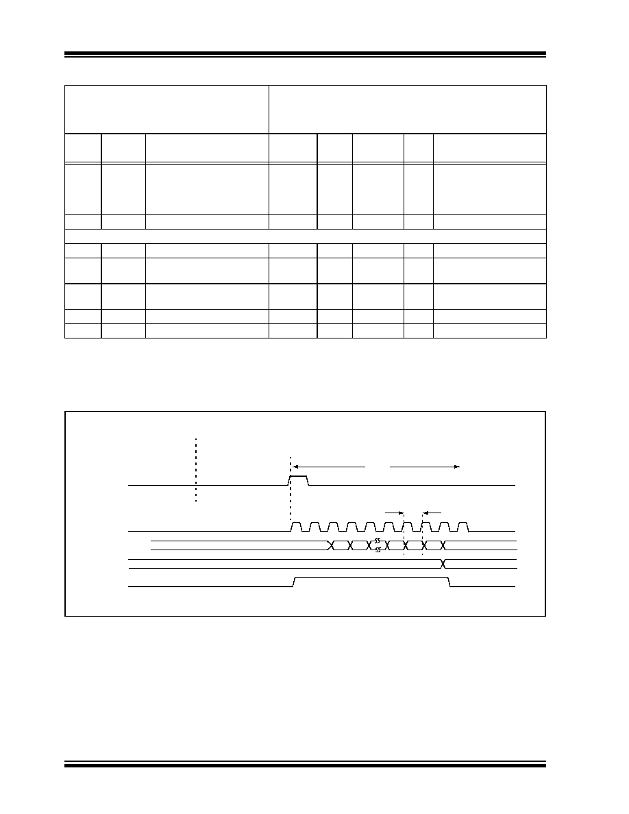
FIGURE 21-20:
A/D CONVERSION TIMING PER INPUT
AD24
EOFF
Offset Error
—
±0.75
<±2.0
LSb
VINL = AVSS = VSS = 0V,
AVDD = VDD = 5V
AD24A EOFF
Offset Error
—
±0.75
<±2.0
LSb
VINL = AVSS = VSS = 0V,
AVDD = VDD = 3.3V
AD25
—
Monotonicity(2)
—
Guaranteed
Dynamic Performance
AD30
THD
Total Harmonic Distortion
-77
-73
-68
dB
—
AD31
SINAD
Signal to Noise and
Distortion
—58
—
dB
—
AD32
SFDR
Spurious Free Dynamic
Range
—-73
—
dB
—
AD33
FNYQ
Input Signal Bandwidth
—
0.5
MHz
—
AD34
ENOB
Effective Number of Bits
—
9.4
—
bits
—
TABLE 21-33: 10-BIT HIGH-SPEED A/D MODULE SPECIFICATIONS (CONTINUED)
AC CHARACTERISTICS
Standard Operating Conditions: 3.3V and 5.0V (±10%)
(unless otherwise stated)
Operating temperature
-40°C
≤ TA ≤ +85°C for Industrial
-40°C
≤ TA ≤ +125°C for Extended
Param
No.
Symbol
Characteristic
Min.
Typ
Max.
Units
Conditions
Note 1:
Because the sample caps will eventually lose charge, clock rates below 10 kHz can affect linearity
performance, especially at elevated temperatures.
2:
The A/D conversion result never decreases with an increase in the input voltage, and has no missing
codes.
TAD
A/D Data
ADBUFxx
90
210
Old Data
New Data
CONV
A/D Clock
Trigger Pulse
Tconv
发布紧急采购,3分钟左右您将得到回复。
相关PDF资料
PIC16CR76T-I/SO
IC PIC MCU 8KX14 28SOIC
PIC18LF24K22-I/MV
IC PIC MCU 16KB FLASH 28UQFN
PIC18LF24K22-I/ML
IC PIC MCU 16KB FLASH 28QFN
PIC16CR76T-I/ML
IC PIC MCU 8KX14 28QFN
PIC16F627-04/P
IC MCU FLASH 1KX14 COMP 18DIP
PIC18F45J10-I/ML
IC PIC MCU FLASH 16KX16 44QFN
PIC18F24K22-I/ML
IC PIC MCU 16KB FLASH 28QFN
PIC16CR76-I/SS
IC PIC MCU 8KX14 28SSOP
相关代理商/技术参数
PIC18F13K50-I/P
制造商:Microchip Technology Inc 功能描述:20 Pin 8 KB Flash 512 RAM 15 I/O 10
PIC18F13K50-I/SO
功能描述:8位微控制器 -MCU 8KB Flash 512 RAM 15 I/O 10-B ADC USB 2.0 RoHS:否 制造商:Silicon Labs 核心:8051 处理器系列:C8051F39x 数据总线宽度:8 bit 最大时钟频率:50 MHz 程序存储器大小:16 KB 数据 RAM 大小:1 KB 片上 ADC:Yes 工作电源电压:1.8 V to 3.6 V 工作温度范围:- 40 C to + 105 C 封装 / 箱体:QFN-20 安装风格:SMD/SMT
PIC18F13K50-I/SO
制造商:Microchip Technology Inc 功能描述:20 Pin 8 KB Flash 512 RAM 15 I/O 10
PIC18F13K50-I/SS
功能描述:8位微控制器 -MCU 8KB Flash 512 RAM 15 I/O 10-B ADC USB 2.0 RoHS:否 制造商:Silicon Labs 核心:8051 处理器系列:C8051F39x 数据总线宽度:8 bit 最大时钟频率:50 MHz 程序存储器大小:16 KB 数据 RAM 大小:1 KB 片上 ADC:Yes 工作电源电压:1.8 V to 3.6 V 工作温度范围:- 40 C to + 105 C 封装 / 箱体:QFN-20 安装风格:SMD/SMT
PIC18F13K50-I/SS
制造商:Microchip Technology Inc 功能描述:8-Bit Microcontroller IC
PIC18F13K50T-I/SO
功能描述:8位微控制器 -MCU 8KB Flash 512 RAM 15 I/O 10-B ADC USB 2.0 RoHS:否 制造商:Silicon Labs 核心:8051 处理器系列:C8051F39x 数据总线宽度:8 bit 最大时钟频率:50 MHz 程序存储器大小:16 KB 数据 RAM 大小:1 KB 片上 ADC:Yes 工作电源电压:1.8 V to 3.6 V 工作温度范围:- 40 C to + 105 C 封装 / 箱体:QFN-20 安装风格:SMD/SMT
PIC18F13K50T-I/SS
功能描述:8位微控制器 -MCU 8KB Flash 512 RAM 15 I/O 10-B ADC USB 2.0 RoHS:否 制造商:Silicon Labs 核心:8051 处理器系列:C8051F39x 数据总线宽度:8 bit 最大时钟频率:50 MHz 程序存储器大小:16 KB 数据 RAM 大小:1 KB 片上 ADC:Yes 工作电源电压:1.8 V to 3.6 V 工作温度范围:- 40 C to + 105 C 封装 / 箱体:QFN-20 安装风格:SMD/SMT
PIC18F14K22-E/ML
功能描述:8位微控制器 -MCU 16KBFlash 512byteRAM 256bytesEEPROM
RoHS:否 制造商:Silicon Labs 核心:8051 处理器系列:C8051F39x 数据总线宽度:8 bit 最大时钟频率:50 MHz 程序存储器大小:16 KB 数据 RAM 大小:1 KB 片上 ADC:Yes 工作电源电压:1.8 V to 3.6 V 工作温度范围:- 40 C to + 105 C 封装 / 箱体:QFN-20 安装风格:SMD/SMT